Thin Films and Surfaces

We modify surfaces in the nanometre range through coatings and by producing polymer-based microfluidics systems.

Our research group

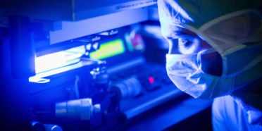
We develop thin surfaces (several nanometres (1nm = 10-9m) to several 100nm layer thickness) using physical vapour deposition (PVD, electron beam evaporation and sputtering) as well as spin and dip coating. Lithography and etching processes enable us to structure surfaces in the micrometre range. We have an ISO 6 class clean room available for these tasks.

Range of services

Our expertise and infrastructure is available to external partners for student theses, research projects or joint projects funded by third parties. Please contact us if you require further details.

Areas of expertise

We are a partner with expertise in the following areas:

Development and production of thin layers

Procedures:

  • Electron beam evaporation
  • Sputtering
  • Spin and dip coating

Areas of application:

  • Metallic layers
  • Dielectric layers for optical applications
  • Polymer coatings
  • Perovskite layers for solar cells
  • Electrodes for biomedical applications

Processes for micro-structuring

Procedures:

  • UV-lithography for four-inch wafer
  • Wet chemical etching methods
  • Production of polymer structures with a thickness of several hundred micrometres

Areas of application:

  • Planar micro-electrodes
  • Polymer-based microfluidics systems
  • Structuring of conducting polymers

Infrastructure

ISO 6 class clean room

White room:

  • Electron beam evaporation for producing thin layers
  • Sputtering unit for producing thin layers
  • Diffusion furnace for thermal oxidation of silicon
  • Plasma system (N2, O2, Ar) for cleaning and modifying surfaces
  • Analytics: Mechanical probe, reflectometer
  • Equipment for carrying out microfluidics experiments

Yellow room:

  • Spin-coater
  • Mask aligner for UV lithography
  • Wet bench for etching processes

Outside the clean room:

  • Dip-coating equipment
  • Scanning force microscopy
  • Ellipsometer
  • Glow discharge spectroscopy GDOES
  • FT-IR with ATR

Contact

Contact us or meet our experts in person at various events. Collaboration produces win-win outcomes for everyone concerned – your company, society and the university.